

Work Package WP1 Leader
Robert Kucharski, PhD, Eng.
Institute of High Pressure Physics of the Polish Academy of Sciences (IHPP PAS)
Main Objectives
The primary objective of package WP1 is to develop and scale the technology of ammonothermal GaN crystal growth and advanced surface processing (wafering), enabling the production of 4-inch GaN substrates characterized by unprecedented structural quality (exhibiting the Borrmann effect) and low electrical resistivity.
Key tasks carried out within this package include:
- Optimizing growth chamber geometry in ammonothermal autoclaves, supercritical fluid mass transport, and pressure-temperature profiles.
- Developing an innovative methodology for seed expansion through lateral growth and seed joining (tiling).
- Advancing multi-wire slicing, chemical-mechanical polishing (CMP), and epi-ready surface preparation for epitaxy.
Technological Expansion Routes
To achieve 4-inch GaN substrates, two complementary technological routes are pursued:
- Monolithic route (monolithic enlargement): lateral expansion of a single seed crystal.
- Segmented route (tiling route): joining shorter seed crystals into a single continuous seed platform.
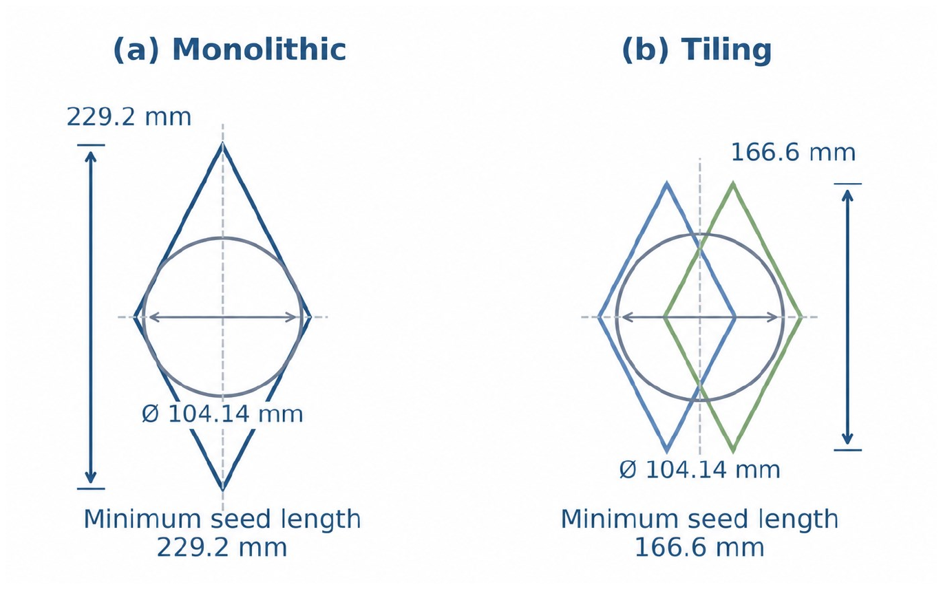
Fig. 1. Comparison of the monolithic and tiling routes toward 4-inch GaN crystals.
The tiling approach reduces the minimum required initial seed length from 229.2 mm to 166.6 mm. This requirement falls comfortably within the range of long GaN seeds (180–218 mm) already synthesized at IHPP PAS.
Results and Current Activities
- Synthesis of Long Seeds: Stable GaN seeds measuring 180–218 mm were successfully synthesized by precise joining of shorter crystal segments. These seeds serve as the foundation for lateral enlargement in high-pressure autoclaves.
- Growth Zone Modification: Novel crystallization zone configurations were engineered and implemented in autoclaves to minimize thermal and mechanical stress during growth.
- Structural Analysis: Detailed investigations into defect distributions and crack propagation in enlarged crystals were carried out, optimizing nucleation conditions at segment boundaries.
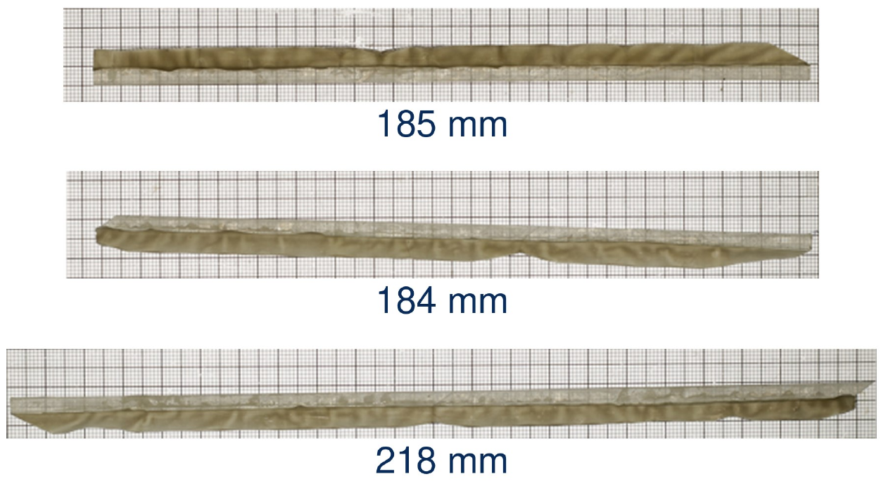
Fig. 2. Examples of long GaN seeds (180–218 mm) prepared for lateral enlargement processing.
Next Steps
- Scaling the lateral expansion process on joined seed platforms to reach target 4-inch diameters.
- Improving CMP recipes to achieve atomic-level surface smoothness across large-area substrates.
- Comprehensive structural and electrical qualification of pilot 4-inch GaN substrates for epitaxial runs in WP2 and WP3.