

Work Package WP2 Leader
Tomasz Sochacki, PhD, Eng.
Institute of High Pressure Physics of the Polish Academy of Sciences (IHPP PAS)
Main Objectives
Research package WP2 focuses on the development of advanced vertical power diodes in a GaN-on-GaN architecture. The use of native, highly crystalline gallium nitride substrates dramatically reduces dislocation density, which is critical for attaining ultra-high breakdown voltages and minimizing reverse leakage currents.
The scope of work encompasses:
- Optimizing epitaxial growth of thick, ultra-pure drift layers using MOVPE and HVPE techniques.
- Precise acceptor doping (Mg) and dopant activation via Ultra-High Pressure Annealing (UHPA).
- Establishing reproducible fabrication processes for p- and n-type ohmic and Schottky barrier contacts.
- Designing and fabricating edge-termination structures and JBS (Junction Barrier Schottky) diodes.
Investigated Device Architectures
Within the package, three primary diode configurations sharing a common n-type substrate and drift layer are developed and benchmarked:
- Schottky Barrier Diodes (SBD): providing ultra-fast switching speeds and low forward voltage drop.
- p-n Junction Diodes: offering superior high-voltage reverse blocking capabilities.
- p-i-n Diodes: optimized for tailored electric field management within the intrinsic region.
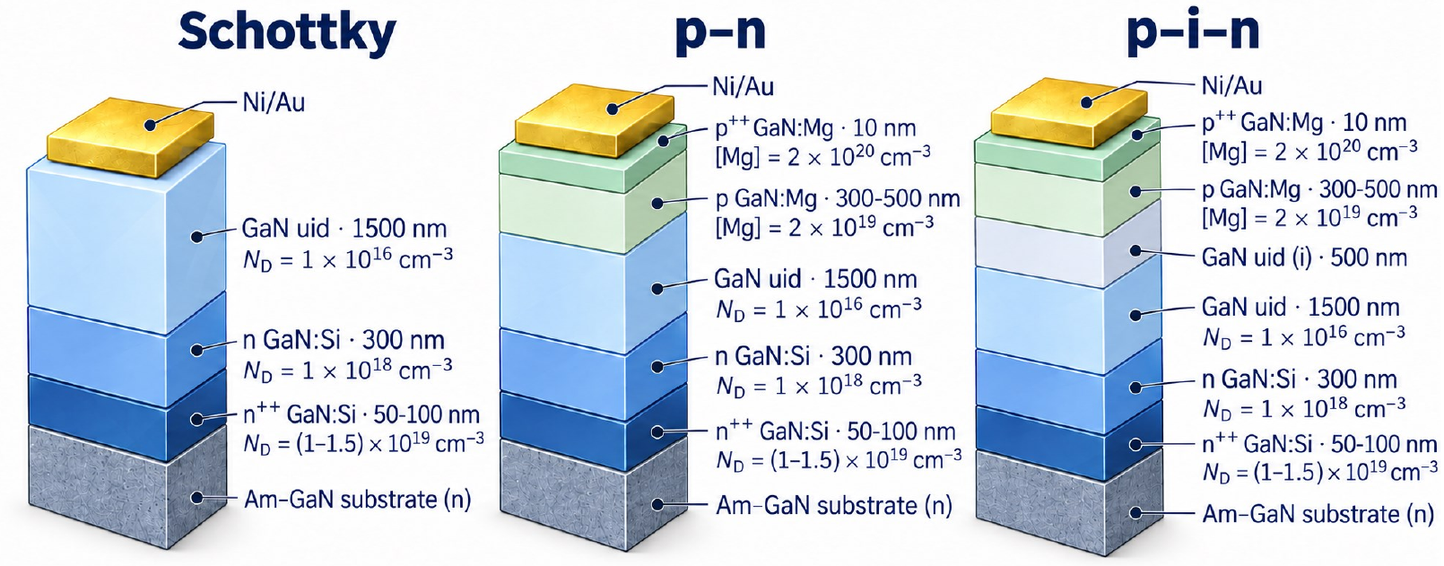
Fig. 1. Architecture of test structures: Schottky, p-n, and p-i-n diodes sharing a common native substrate and drift layer.
Results and Progress
- Characterization of Am-GaN Substrates: A comprehensive electrical characterization suite was performed on 2-inch ammonothermal substrates (Hg-probe C-V, microwave resonators, SiPDR resistivity mapping). A clear correlation between decreasing resistivity and increasing net donor concentration ($N_D - N_A$) was confirmed.
- Fabrication of Test Structures: MOVPE epitaxy on Am-GaN substrates and HVPE on dedicated carriers were successfully executed, producing series of test diode structures for transport parameter calibration.
- Passivation Dielectric Evaluation: Nine dielectric variations deposited via PECVD and ALD were evaluated for dielectric breakdown strength. PECVD-grown SiN layers exhibited the highest breakdown voltages (53–89 V) and were selected for uniformity validation.
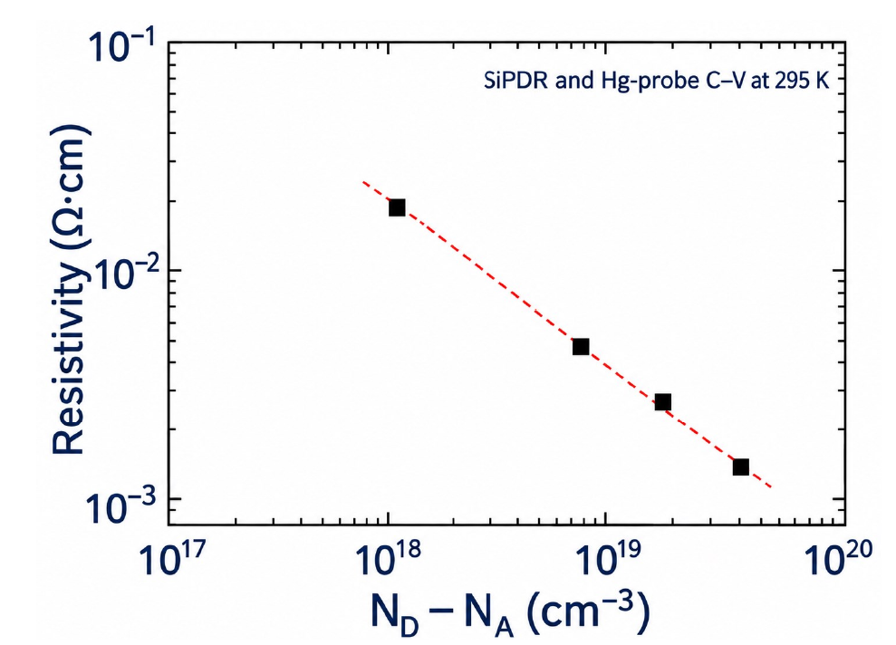
Fig. 2. Resistivity of Am-GaN substrates as a function of net donor concentration ($N_D - N_A$), measured by SiPDR and Hg-probe C-V at 295 K.
Upcoming Milestones
- Precision dicing of 2-inch substrates into $11 \times 11\text{ mm}$ working dies from qualified uniform zones.
- Implementation of ion implantation and dopant activation runs in high-pressure UHPA reactors.
- Experimental evaluation of dynamic and high-temperature performance metrics of prototype vertical power diodes.